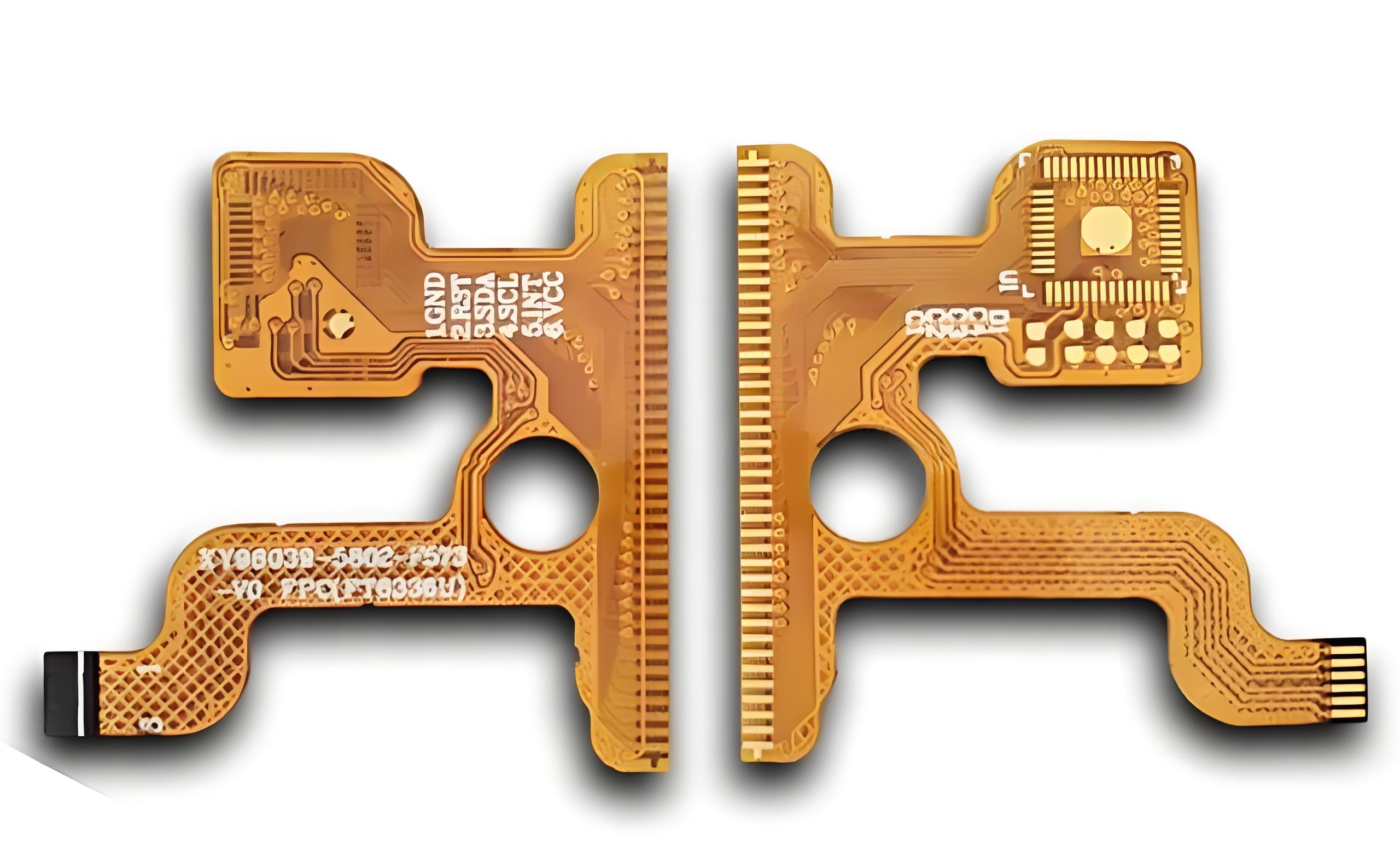


We specialize in using Altium Designer, Cadence and Protel design PCB boards for 1-6 layers, including FR-4 boards 、 aluminum substrate boards and FPC bords,We will been still to be a leader and construction of our product supplier specialists,
In Shenzhen and surrounding areas, there are many professional PCB manufacturers who can easily carry out mass production of PCB boards。
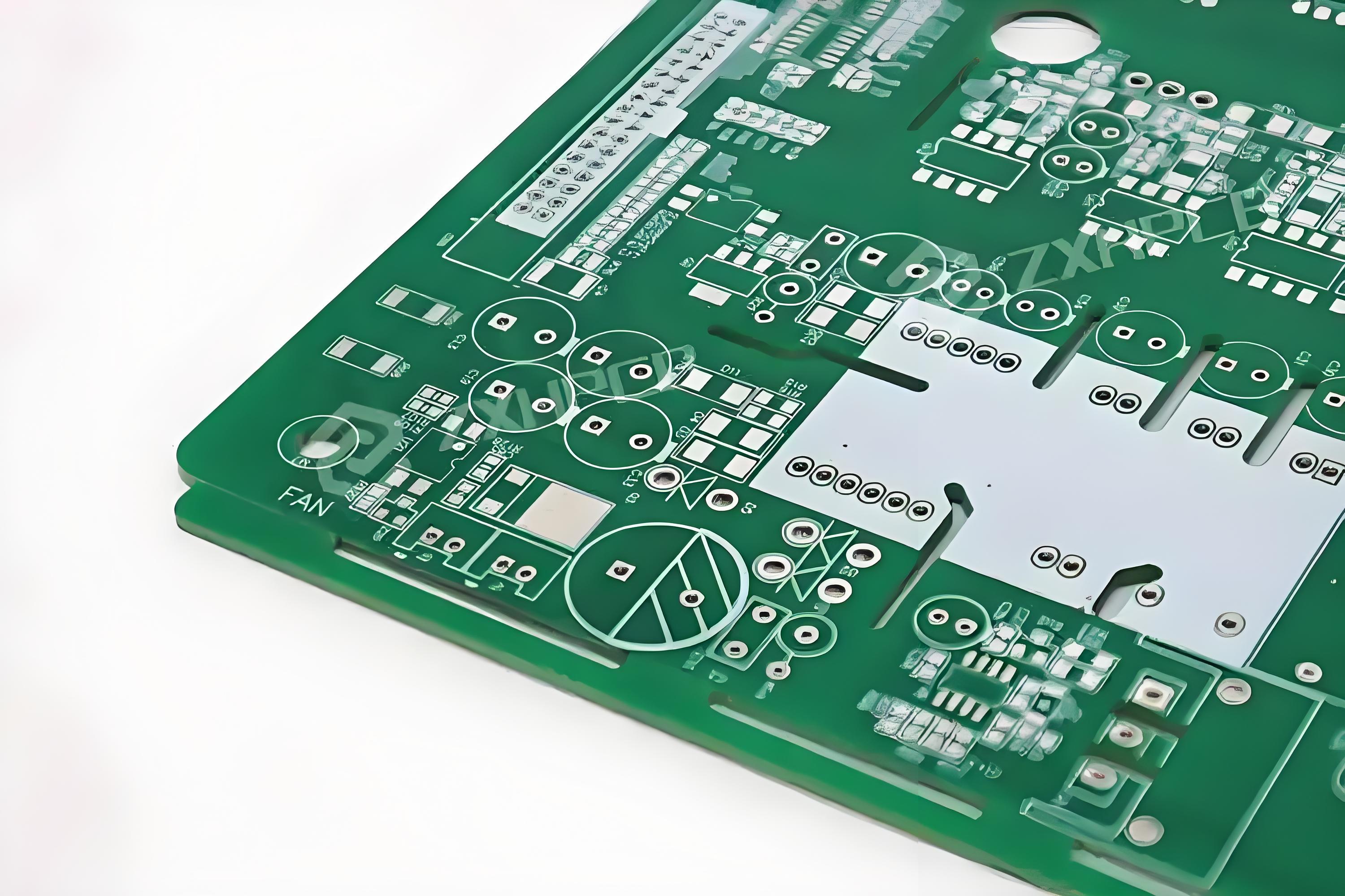
Core manufacturing capability parameters of our PCB boards:
- Layer Count & Dimensions: Supports up to 64-layer ultra-high-layer PCBs, with a maximum board thickness of 5mm and maximum panel size of 656×586mm; standard high-multilayer production covers 6 to 32 layers.
- Line Width/Spacing: Minimum line width/spacing can reach 0.09/0.09mm (3.5mil); BGA local line width can be as small as 3mil.
- Hole Size & Drilling: Mechanical drilling supports diameters from 0.15mm to 6.3mm; 0.1mm micro‑vias are in mass production (limited to 2–12 layers, board thickness ≤1mm). HDI technology supports laser drilling (hole size 0.075–0.15mm) with resin plugging and cap plating.
- Surface Finish: For 6–64‑layer boards, immersion gold (ENIG) is offered as a free standard finish, with gold thickness typically 2µ”, ensuring flat pads, oxidation resistance, and suitability for BGA soldering.
Key Process Advantages
- Positive‑process (Tenting): The entire line adopts positive‑process instead of negative‑process. Although the workflow is longer, it significantly improves circuit precision, fundamentally eliminates “bad hole” risks, and ensures high‑density routing reliability.
- Via‑in‑pad (VIP): For high‑multilayer boards, via‑in‑pad with resin plugging and cap plating is provided as a free standard. Vias are placed directly on the pads with flat surfaces, resolving BGA solder‑leakage and cold‑joint issues, and effectively increasing routing space.
- HDI & Blind/Buried Vias: Capable of manufacturing 4–32‑layer (1‑3 order) HDI boards. Uses laser drilling and electroplated filling technology to meet miniaturization demands in consumer electronics, AI servers, and other applications.
- Impedance Control: Supports custom impedance designs. CAM engineering can automatically adjust line width and spacing based on the stack‑up, with impedance tolerances controlled within high‑industry standards.
Equipment & Quality Control System
- Advanced Equipment: Key production lines are equipped with LDI laser direct‑imaging equipment (for improved exposure precision and speed), fully automatic laminating presses, and pulse electroplating (VCP) systems, ensuring layer‑to‑layer alignment accuracy and hole‑wall quality.
- Full‑process Inspection: Implements four‑wire low‑resistance testing, flying probe testing, AOI (automated optical inspection), AVI, and X‑ray non‑destructive inspection. High‑multilayer boards maintain a stable high yield rate.
- Substrate Materials: Uses only A‑grade materials from major suppliers such as Shengyi, Nanya, and KB, ensuring stable dielectric constants and meeting high‑speed signal transmission requirements.
Application Scenarios & Recommendations
- Best‑suited Scenarios: Excellent for R&D prototyping, small‑ to medium‑batch pilot production, and mid‑to‑high‑end applications such as AI servers, 5G communications, and automotive electronics. Offers rapid turnaround (e.g., 6‑14‑layer boards with 48‑hour expedited service).
- Important Notes: For ultra‑high‑layer boards (e.g., >40 layers), managing material expansion/shrinkage and alignment tolerances is challenging. It is advisable to add copper pours in inner‑layer open areas to balance stress. For high‑voltage or high‑current power applications, careful evaluation of dielectric thickness limitations is required.
- Overall Positioning: Our manufacturing capability ranks among the industry’s top tier in terms of turnaround speed and cost‑effectiveness, with a high degree of process standardization. However, for specialized applications with military‑grade or extreme‑reliability requirements, additional validation against relevant certifications is still necessary.