


Hardware circuit design is a critical part of electronic product development and typically involves the following steps:
1. Requirement Analysis
- Identify the product’s functional requirements, performance metrics, power consumption, and operating environment.
- Draft an initial technical specification to define the goals and constraints of the hardware design.
2. Solution Design
- Overall Design: Select appropriate chips (MCU, FPGA, SoC, etc.), power solutions, and communication interfaces.
- Module Division: Divide the system into functional modules (e.g., power supply module, sensor interface module).
- Component Selection: Choose suitable components (resistors, capacitors, transistors, etc.) based on functional requirements.
3. Schematic Design
- Create a circuit schematic using design software (e.g., Altium Designer, Cadence, KiCAD).
- Ensure circuit correctness, including signal connections, impedance matching, and power distribution.
- Add necessary protection circuits (e.g., overcurrent protection, ESD protection).
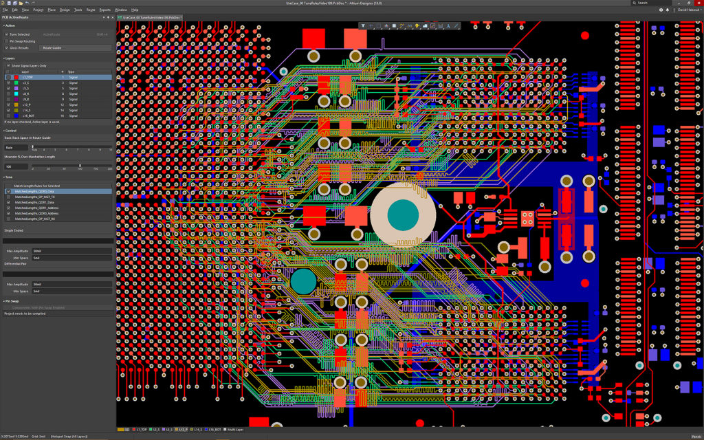
4. PCB Design
- PCB Layout: Place components on the PCB based on the schematic.
- PCB Routing: Complete signal and power line routing while ensuring signal integrity and electromagnetic compatibility (EMC).
- Layered Design: For multilayer PCBs, allocate power, ground, and signal layers appropriately.
5. Simulation and Validation
- Use simulation tools (e.g., SPICE, HFSS) to validate circuit functionality and performance.
- Focus on key modules such as power stability and RF signal quality.
6. Fabrication and Soldering
- PCB Fabrication: Submit design files to a PCB manufacturer for prototyping or mass production.
- Component Soldering: Assemble components through manual soldering or automated pick-and-place machines.

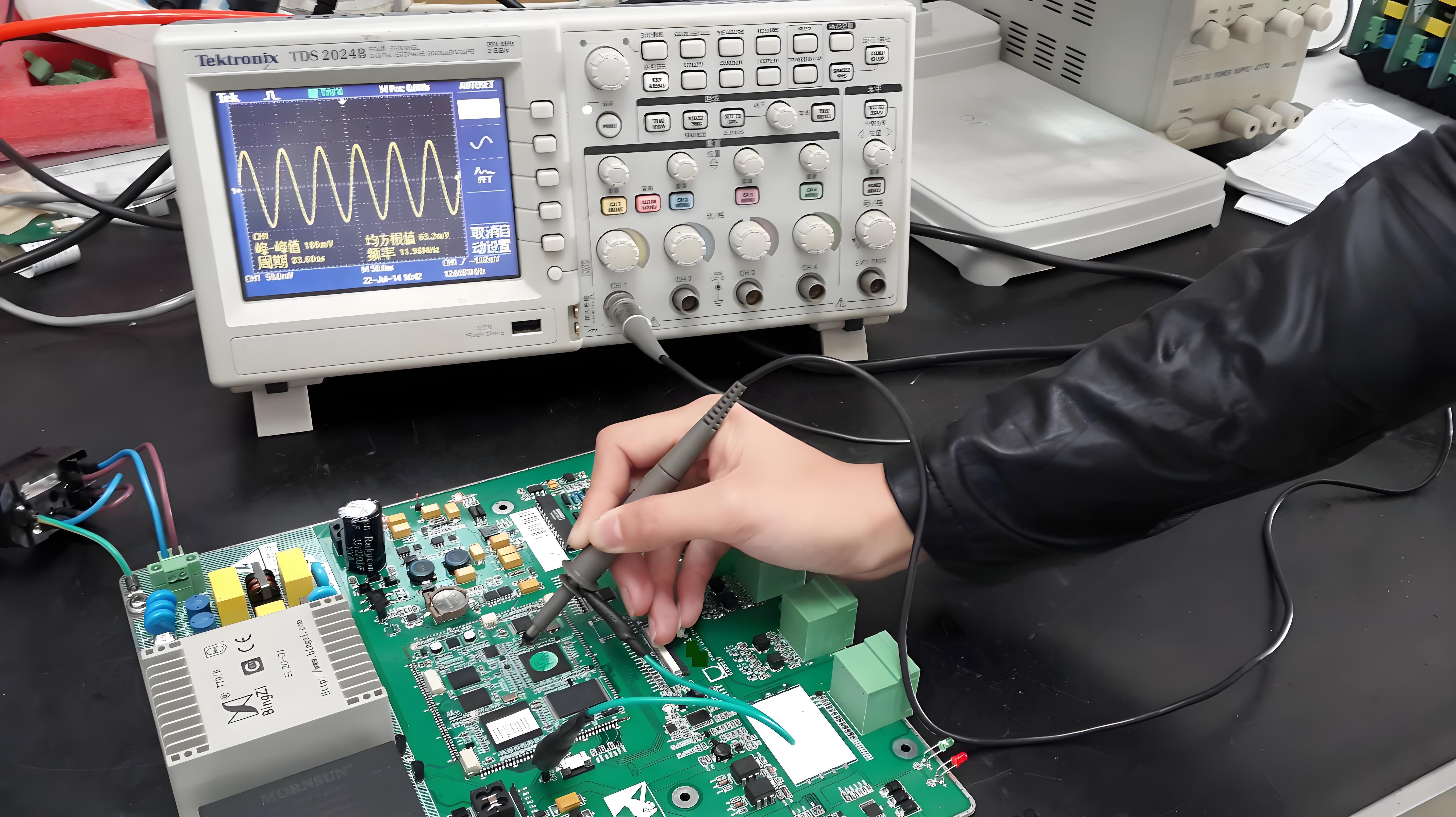
7. Testing and Debugging
- Use testing tools like oscilloscopes and multimeters to verify the circuit board’s functionality and performance.
- Identify issues, modify the design, and repeat prototyping until validation is successful.
8. Finalization and Mass Production
- Confirm the design’s stability and reliability, and finalize the hardware design.
- Transfer the finalized hardware design to the production line for mass manufacturing.